


Buena Vista Images/DigitalVision via Getty Images
KLA’s (NASDAQ:KLAC) process control revenue outgrew WFE, growing at 19% from 2018 to 2021 compared to 15.8% for the WFE sector. Chart 1 shows KLAC’s revenues between 2010 and 2021. It also shows its market share reaching 54.4% in 2021, according to our report entitled “Metrology, Inspection, and Process Control in VLSI Manufacturing.”

The Information Network
Chart 1
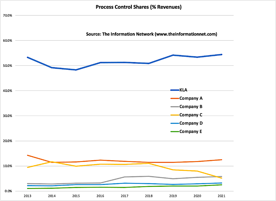
KLAC’s share was more than 4x its nearest competitor and essentially achieved the team’s 2023 target of 53.5% share two years early. Chart 2 shows KLAC’s share and that of the next five competitors. KLA gained share against competitors in 2021.
The Information Network
Chart 2
Comparing revenues for three quarters of 2022 vs. three quarters of 2021 is shown in Chart 3. KLAC led the top equipment companies with 33.1%, a factor of 3X greater than the mean for all companies of 11.2%.

The Information Network
Chart 3
In Table 1, I present KLAC’s revenue and peers by chip type for 2021. KLA’s generated 56% of revenue from foundries and 11% from logic companies in 2021.

The Information Network
KLA’s Tailwinds
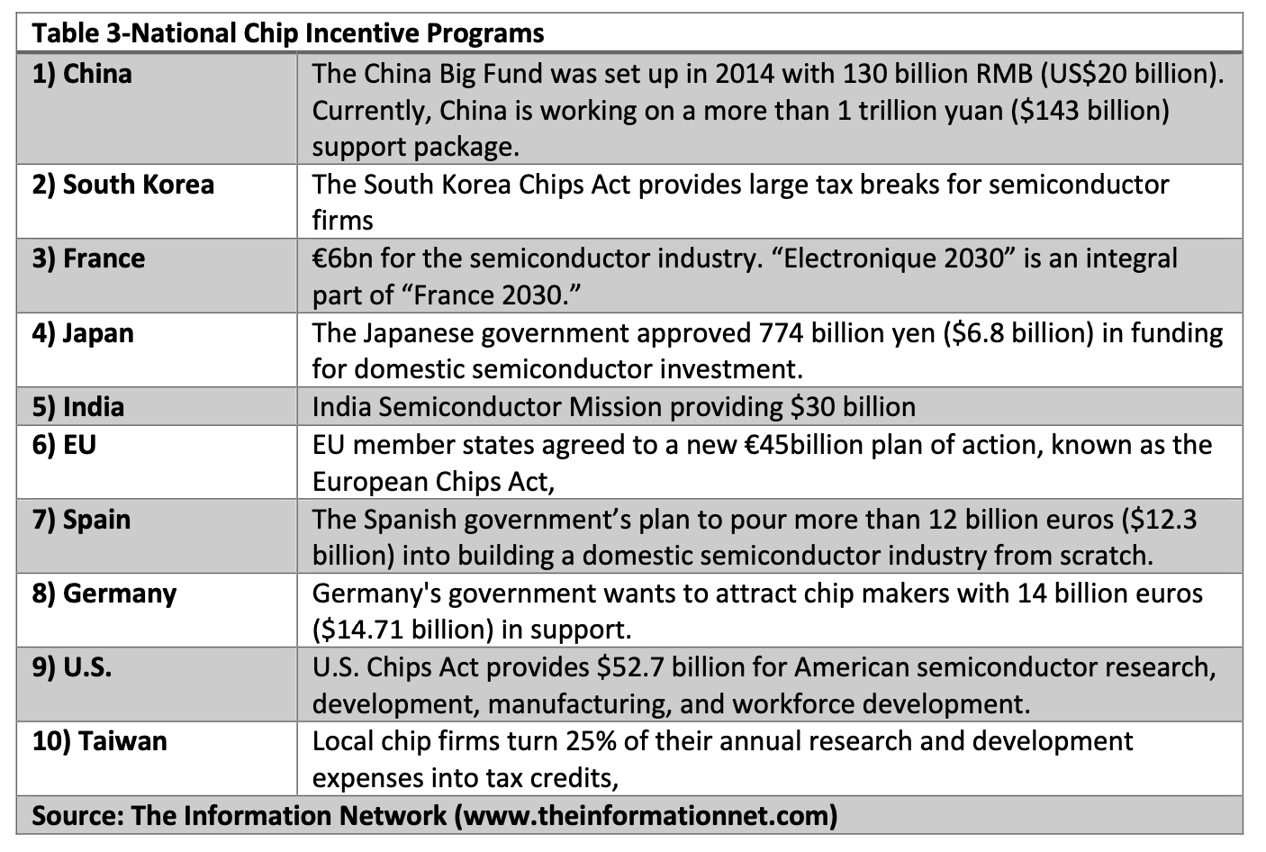
As I will discuss below, while the CHIPS Act in the U.S. has been the most publicized of all national chip incentive programs, there are in fact nine other countries that now offer incentives to semiconductor companies to build fabs in their country.
Most of the fabs to be built will be a foundry or logic chip manufacturer, and many foundries make logic chips, such as those from fabless companies AMD (AMD) and Nvidia (NVDA) made by Taiwan foundry TSMC (TSM). Alternatively, Intel (INTC) makes its own logic chips in its own fab. These represent a tailwind for KLAC.
Another tailwind for KLAC is the greater need for metrology/inspection equipment at small nodes, such as <10nm, than larger nodes. The reason is simple. Smaller-node wafers are priced higher than larger node, and a killer defect or glitches in the manufacturing line will result in greater revenue losses for the manufacturer.
As an example, ASPs (average selling prices) for wafers at 3nm are $20K, increasing to $25K for the 2nm node. This compares to just $3K for a 28nm node wafer. As discussed below, nearly all the foundries that will be built by TSMC, Samsung Electronics (OTCPK:SSNLF), and Intel under national chip incentive programs will be built to process <10nm node wafers.
Semiconductor Industry and Basis for National Chip Incentive Programs
It’s important to recognize that the purpose of the U.S. CHIPS Act is not only to bring semiconductor manufacturing back to the U.S., compete with China, increase innovation and enable the production of leading-edge <10nm node chips in the U.S., but to boost national security. I discussed the U.S. CHIPS Act extensively in an Oct. 31, 2022, Seeking Alpha article entitled “$53 Billion Of Handouts For CHIPS Act And U.S. Forecast To Gain Just 1% Share By 2025!”
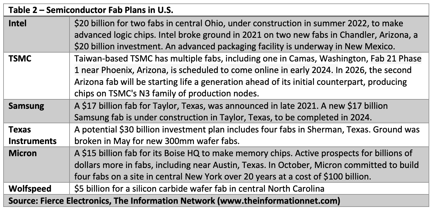
Table 2 shows presents a list of chip companies that are in the process of building these fabs.
The Information Network
Geopolitical factors in the past few years have accentuated the resolve of other countries to boost their own national security. Now the U.S. faces competition from other countries, as they’re offering inventive programs similar to the CHIPS Act.
New Fabs In U.S.
Table 3 shows the theses programs, a timeline, and date, which I detail below.
The Information Network
New Fabs Outside U.S. (Excluding China)
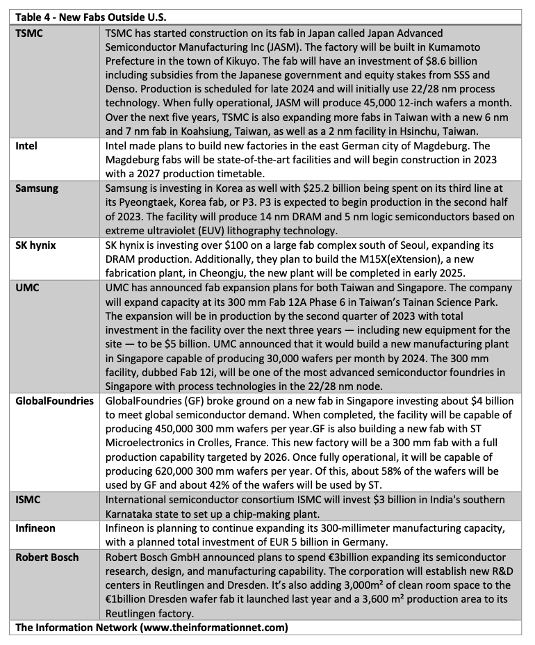
Table 4 shows new fabs planned that will be benefiting from national chip incentive programs.
The Information Network
KLA Stock Performance vs Peers
Chart 4 shows % change in share price for ASML (ASML), Applied Materials (AMAT), KLAC, Lam Research (LRCX), and Tokyo Electron (OTCPK:TOELY) for a one-year period. KLAC has exhibited the best share performance.
AMAT, LRCX, and TOELY have similar percent share price change, which is astonishing since all three companies are strong competitors of each other in deposition and etch equipment, and what is positive news for AMAT should be negative news for LRCX and TOELY. This suggests that these semiconductor stocks are traded as a sector and not on an individual basis.
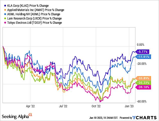
YCharts
Chart 4
Further illustrating the superior performance of KLA, Chart 9 compares Gross Profit Margin for the one-year period.
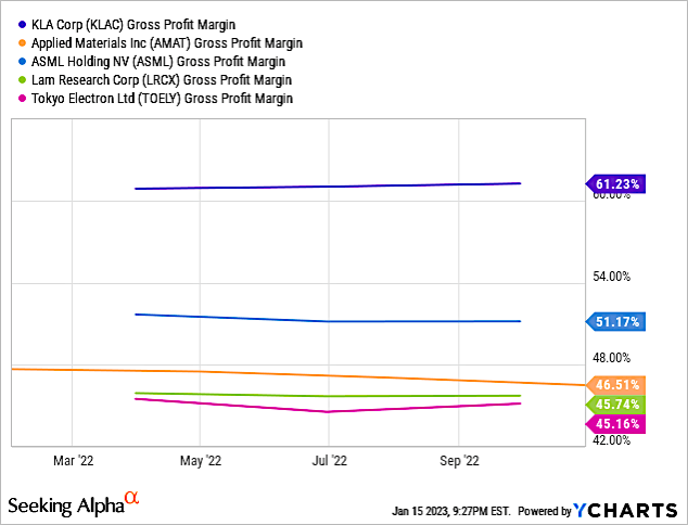
YCharts
Chart 5
KLAC will benefit from the numerous National Chip Inventive Programs, since most of the new fab plans are foundry and most of them from TSMC, Samsung Electronics, and Intel will be making chips at the <10nm nodes.
The need for metrology/inspection equipment increases as semiconductor technology nodes decrease. The reason is that ASPs for wafers at 3nm are $20K, increasing to $25K for the 2nm node. This compares to just $3K for a 28nm node wafer.
At smaller nodes, any defect that could ruin a 3nm wafer represents a bigger loss to the company than a wafer made at 28nm. These killer defects are uncovered during metrology and inspection of wafers using equipment from KLAC.
Editor’s Note: This article discusses one or more securities that do not trade on a major U.S. exchange. Please be aware of the risks associated with these stocks.
Be the first to comment