

ratpack223
Introduction
Semiconductor logic devices have transitioned from planar transistors to FinFET transistors at the 16-nm process node as a means of lowering leakage, improving scalability, bolstering drive currents, and accelerating switching times. The FinFET manufacturing technology has scaled well from 22-nm chips all the way down to 5-nm chips.
The gate-all-around (“GAA”) is the next-generation semiconductor process technology, offers two unique advantages over FinFETs. First, GAA transistors solve many challenges associated with the leakage current since GAA channels are horizontal. Second, GAA transistors are surrounded by gates around all four sides. That improves the structure of a transistor by enabling a gate to contact all four sides of a transistor compared to the three sides in the current FinFET process.
GAA transistor architecture is 90% similar to FinFET, and the remaining 10% difference comes from stacking horizontal nanosheets on top of one another.
The evolution of different types of FET devices is shown in Chart 1.
Samsung
Chart 1
Deposition Processes
In a planar device, the metal film could be deposited top-down by PVD (sputtering). For FinFETs, it is very difficult to form a conformal film on the sidewall of the fins using this anisotropic deposition technique. CVD technique has much better isotropy than PVD and is able to meet the requirement of FinFETs.
For the GAA device structure, the deposition of HKMG requires precision in atomic levels. The ALD technique offers a good control for layer thickness of HfO2 and TiN. The fins are separated by only 10nm. In that space, a high-k material, a gate metal and a metal that defines the work function of the transistor are deposited.
For GAA FETs, however, both PVD and CVD will be phased out from the deposition of gate layers, replaced by atomic layer deposition (“ALD”), according to our report entitled Global Semiconductor Equipment: Markets, Market Shares and Market Forecasts. A key challenge with GAAFETs is the need to deposit the multi-layer gate oxide and metal gate stacks around the tiny 10 nm channels.
Applied Materials’ (NASDAQ:AMAT) high-vacuum Integrated Materials Solution system (Chart 2) for the gate oxide stack integrates ALD, thermal steps, plasma treatment steps, and metrology. According to AMAT, these stacks are highly complex and can contain upwards of 7 layers. These include the Interface and high-k layers and the metal gate layers. Interface and high-k scaling is critical to gate oxide reduction which boosts the drive current. The metal gate is tuned to ensure the transistor has the correct work function which determines the threshold voltage.
Applied Materials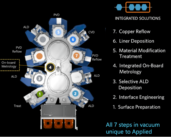
Chart 2
The National Institute of Standards and Technology (NIST) evaluated a technique called ion beam deposition (“IBD”) and compared films also made with ALD. Chart 3 shows that IBD oxide has a superior breakdown field (2,000-3,000 MV/m) to that of ALD oxide (1,300 MV/m). Furthermore, the breakdown field was found to be independent of the junction area, strongly suggesting the absence of pinholes.
NIST
Chart 3
The breakdown voltage of an insulator is the minimum voltage that causes a portion of an insulator to experience electrical breakdown and become electrically conductive. At that point, a FinFET or GAA will fail.
The conclusions drawn by scientists at NIST are that ion beam deposition is capable of depositing very high-quality oxides at room temperature. The technique allows sub-nanometer control over the film thickness. The biased target version of IBD is able to produce sharp interfaces with minimal interdiffusion.
Denton’s Deposition Technology
Denton Vacuum has developed ion beam deposition processes of thin films used in FinFET and GAA processes for a semiconductor customer. Data show that low pressure ion beam deposition and etch provides ultra-smooth films with exceptional uniformity and sub-Angstrom thickness precision:
- <2Å rms roughness
- <0.1Å nominal thickness control
- <0.5% thickness non-uniformity
- <0.5% oxidation non-uniformity
- Homogeneous thin films
- Low damage – no plasma strike exposure
For Ion beam deposition, Denton biases the target to 1) control the energy levels of ions bombarding the target, 2) eliminate bombarding shields and other parts of the ion beam system which creates contamination, and 3) increase deposition rate over traditional ion beam deposition. For ion beam etch, Denton biases the substrate to control the level of energy hitting the substrate, this is particularly important for low damage etch of advanced devices under 7nm.
Table 1 compares the properties of the films measured during this devaluation of deposition methods for FinFETs and GAA.
Denton Vacuum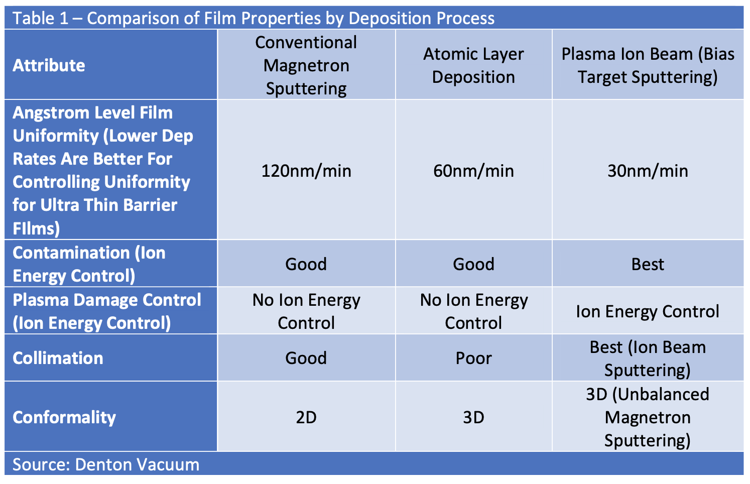
As fill materials change, the requirements on liners (or requirements to even have liners/barriers) will also change. The processes associated with these materials will present advantages and disadvantages for different integration schemes, like dual-damascene, single-damascene, fully-self-aligned integration, and even subtractive metallization. Low pressure ion beam deposition and etch provides exceptional uniformity and sub-Angstrom thickness precision.
Denton’s bias target ion beam sputtering technology is unique, providing collimated, ultra-uniform films for fill and planarization.
In addition to the better breakdown voltage of IBD films is desirable for GAA, two other parameters of thin films are also important – conformal coverage capability and low interface state density of gate dielectric.
- Conformal – There are techniques available to make ion beam sputtering films conformal as required.
- Low interface state density – Denton’s proprietary bias target sputtering enables ion energy control for smooth, defect free interfaces.
Investor Takeaway
While Samsung (OTCPK:SSNLF) is using GAA for its 3nm chips, TSMC (TSM) won’t use it until it hits 2nm production which could be in 2025. TSMC will continue to employ FinFET transistors on its 3nm chips which cover only three sides of the channel. Intel (INTC) will also use GAA starting in 2024. Intel calls its GAA transistors RibbonFET.
I discussed the logic roadmaps for these companies in my January 9, 2023, Seeking Alpha article entitled “TSMC: My Top Pick In 2023 As It Dominates Samsung Electronics And Intel Foundries.” Table 2 illustrates the FinFET and GAA roadmaps of the three companies.
The Information Network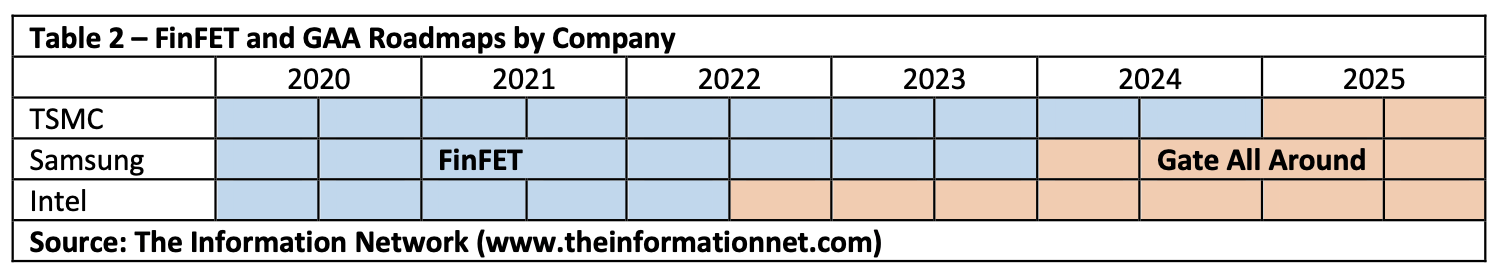
Semiconductor FinFET manufacturers continue to optimize processes and materials as they develop manufacturing capabilities for FinFETs and GAA as dimensions drop below the 3nm node. At these dimensions, the price of a silicon wafer containing these chips gets increasingly expensive, as shown in Table 3.
The Information Network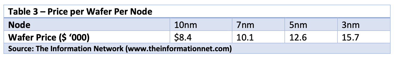
Applied Materials, to much fanfare in its 2021 Logic Master Class introduced its 7-module system that includes ALD for deposition. At a significantly lower system cost, Denton Vacuum’s IBD system has been shown to produce superior films compared to AMAT’s system.
As the three heavyweights in logic chips – TSMC, Samsung, and Intel – move to develop GAA processes for production, equipment that offers best-of-breed capabilities is of paramount importance. Denton’s films have already been demonstrated in the lab and will give AMAT’s ALD solution a run for the money.
I rate AMAT a Sell. The company continues to “talk the talk” by promoting its technology without being able to execute. I have written extensively on how AMAT continues to lose market share against competitors, because it does not have “best of breed” equipment that would GAIN share.
As customers buy more equipment to increase capacity, they will buy more of the competitors’ systems installed and performing, thereby AMAT will lose more share. Readers can learn more in my February 9, 2023, Seeking Alpha article entitled: “Applied Materials: Important Questions Are Still Unresolved Leading Up To Its Next Earnings Call.”
Be the first to comment