

Michael Vi
Today, I will be completing a deep-dive on ASML (NASDAQ:ASML). This company is of irrefutable value to the semiconductor space; without it, the industry would come to a halt. Herein, I provide a brief overview of where the company fits within the semi value chain, outline their business and the products they offer customers, break down their most recent financials, discuss my valuation model, and more.
Note: All monetary values mentioned herein are in millions of Euros.
Over the course of millennia, humanity has propelled itself forward, manipulating our environment in ways that could have never been foreseen in order to propel ourselves to a sustained position at the top of the food chain. Looking back at human progress, there is an embedded “exponentially” to all of it. Arguably the majority of happenings that have had the most impact came into fruition within the last few centuries – an infinitesimally small amount of time in the great scheme of things.
When one thinks of inventions or milestones that have had a drastic impact on said progress, a few things come to mind. Creations like the nail, the wheel, penicillin, the compass, printing presses, the internal combustion engine, the telephone, the internet, the lightbulb, etc., all of these things may pop up. If you stand back and examine these inventions for commonalties, a few factors are apparent. However, one stands out – most of these inventions exist out in the open. Bring up any of them at a dinner party and most people will likely have an understanding of their functionality, their use cases, and the associated impacts that they have on their lives. In contrast however, there are a few innovations that operate under a veil of secrecy, powering the world’s most important industries, yet failing to enter into the common knowledge base of the masses. Lithography is one of these inventions.
The process of Extreme Ultra Violet (EUV) lithography is nothing short of jaw dropping and begs the question: how on earth is it even possible? Read this short description of the process to see what I mean:
An extreme ultraviolet lithography machine is a technological marvel. A generator ejects 50,000 tiny droplets of molten tin per second. A high-powered laser blasts each droplet twice. The first shapes the tiny tin, so the second can vaporize it into plasma. The plasma emits extreme ultraviolet (EUV) radiation that is focused into a beam and bounced through a series of mirrors. The mirrors are so smooth that if expanded to the size of Germany they would not have a bump higher than a millimeter. Finally, the EUV beam hits a silicon wafer—itself a marvel of materials science—with a precision equivalent to shooting an arrow from Earth to hit an apple placed on the moon. This allows the EUV machine to draw transistors into the wafer with features measuring only five nanometers—approximately the length your fingernail grows in five seconds. This wafer with billions or trillions of transistors is eventually made into computer chips.
Crazy right!
But where exactly do lithography processes fit within the chip design process? Bearing in mind that this will be an oversimplified explanation, the process starts off with what is known as a “wafer”, i.e., a thin slice of semiconductor substance such as crystalline silicon, the material that semiconductors themselves are made up of.
The wafer is then coated with a “photoresist”, a.k.a. a light-sensitive chemical. A “mask” is then placed on the wafer, which can be thought of as the stencil for the integrated circuit pattern. Typically this mask is ~4 times larger than the desired intended pattern on the chip. UV will shine through the mask, encoding the desired chip pattern, and make its way through the lithography machine’s optical system, which typically consists of a series of projection lenses that shrink the light down and focus the pattern onto the wafer itself. After the integrated circuit pattern is printed, the system will move slightly and replicate the process across the surface area of the wafer. This process will then be repeated 100+ times, and patterns will be laid atop one another, oftentimes with lithography machines of different specificities, until the final chip design is arrived upon. I skipped several steps here but in short … lithography machines use light to draw nanoscopic patterns on semiconductors inherent to their functionality.
We now understand what lithography is, but how did ASML come to be?
Throughout the ’60s and ’70s, the United States dominated the photolithography market, a phenomenon that Japan was not willing to accept. In order to attempt to remain competitive within the industry, the Japanese government, through the VLSI Research Project, ordered optical manufacturers to catch up to their American counterparts (PerkinElmer and the Geophysics Corporation of America at the time). After putting their noses to the grindstone, Nikon (OTCPK:NINOY)(OTCPK:NINOF) and Canon (CAJ) introduced their first commercial steppers, of which offered superior performance at a much lower price in comparison to American products. As a result, these entities overthrew American competitors to gain the majority of the market share by the end of the ’80s.
A few years later, in 1984, ASML was founded as a joint venture between Philips and ASM International, a Dutch manufacturer. Their early years were far from pretty. Their initial product launch was not gaining traction, and the company was haemorrhaging cash. As a result, 6 years after inception ASM was forced to sell shares to Philips and two banks. ASML was then spun out into its own company shortly thereafter. The launch of their second product, the PAS 5500, fared much better than the first, and as a result, the company was able to move into a more prosperous position. In addition, three big developments within the industry as a whole allowed for them to snap up market share and develop the foundation for the position they find themselves in today.
-
In 2001, the company developed the Twinscan system, a piece of machinery that capitalized on the move towards a two-stage lithography process (i.e., a measurement stage and an exposure stage). The Twinscan would expose one wafer, and in parallel would align the next wafer and ensure its surface is mapped with precision. When imaging was complete on the first, the two stages were then swapped and the next wafer was moved into the exposure position. This innovation essentially removed all overhead time and maximized efficiencies by ensuring wafers were continuously patterned. Due to the complexity of this design, Nikon and Canon were unable to replicate ASML, thus relinquishing more market share to Dutch incumbent.
-
Later that year ASML again innovated with immersion lithography. Typical lithography has an airgap between the wafer and the lens. Immersion lithography on the other hand replaces the air gap with a layer of water, allowing smaller wavelength process nodes to be reached as a result. ASML was able to commercialize on these ideas quicker than competitors with the launch of their AT 1150i machine. Resultantly, ASML had created a device that had much higher numerical aperture than competitors (a measurement of the ability for the machine to gather and focus light). Because of that, customers were able to manufacture layers with smaller features than what was previously possible.
-
Lastly, the company capitalized on the emergence of EUV. After looking for potential avenues for continued innovation, the big chip makers banded behind ASML to direct efforts at the inception of the next stage of lithography, settling on the fact that EUV breakthroughs offered a more enticing proposition than particle-based solutions. As a result, these large chip manufacturers provided ASML with capital to commercialize this technology. With incumbents not partaking in any commendable developments of their own simultaneously, market forces essentially ensured that the throne of EUV would be held by ASML. This competitive position will likely reap sustained rewards going forward, and bar any other technological developments that displace its effectiveness, will be hard-pressed to be disrupted.
If you want more info on how ASML propelled to the top of the lithography market, I would recommend checking out this video
With all of this backstory in mind, what does ASML look like today?
ASML gears products at two different semiconductor industry end-markets, logic chip manufacturers and memory chips manufacturers. Though both essential constituents of the majority of the electronic devices we hold so dear today, they differ in function. Logic chips can be thought of as the “brains” of the electronic devices, whereby they process information in order to complete a task. These include the chips such as CPUs, the central component of the device that calculates and interprets instructions while one is using a device to browse the web, create documents etc., the likes of GPUs, which can process many pieces of data simultaneously, making the technology extremely useful for machine learning, gaming, AI, etc., as alluded to in previous deep-dives pertaining to AMD (AMD) and Nvidia (NVDA), and other hardware such as Neural Processing Units (NPUs) which can be used within a series of deep learning applications, as an example. Memory chips on the other hand are different, and can be used to store data. Different memory chip subsets include the likes of Dedicated Random Access Memory (DRAM) chips, which provide temporary workspaces for data that can be used until the device turned off – i.e., a form of volatile memory, or its counterpart NAND, which is non-volatile memory, and can save data even when the power is removed.
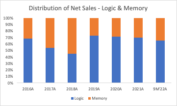
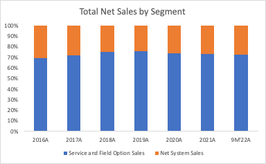
Lithography machines can be used to manufacture both types of machines. As a result, ASML, as of 9M’22A, attributes approximately 65% of their net sales to logic customers, and 35% to memory, a distribution that has fluctuated over the course of the last few years:
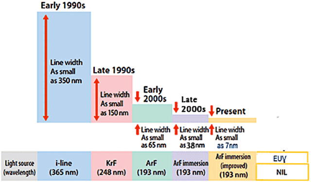
ASML product offerings that they gear at these customers can be placed in three oversimplified buckets, EUV, DUV and Metrology and Inspection. Honing in on DUV and EUV, these products should be thought of with respect to a spectrum of sorts. When ASML was founded, the company’s machines passed electricity through a light that contains mercury, and the required wavelengths were selected therein with an interference filter. This light was capable of creating blue light at 436nm, of which could print features as small as 1000nm. These are typically known as i-line devices. As technological needs evolved, so did the requirements of these lithography machines. A new manner to create light was thus needed – enter Deep Ultraviolet (DUV). Leveraging mixtures of gases that don’t typically combine, scientists were able to apply energy to said mixture to form temporarily excited molecules, of which released excess energy at small wavelengths of light. Using krypton and fluorine, excimer lasers were applied to these gas mixture and started off able to produce light at a wavelength of approximately 248nm, of which can create features down to 80nm in size. Next were ArF machines, further innovated upon with ArFi (ArF immersion), which placed a layer of water between the wafer and the lens in order to increase the numerical aperture, and used a combination of argon and fluoride to produce light with a wavelength of 193nm, a value that now allows for features of up to 38nm to be produced. Finally, EUV machines were then created, using wavelengths of light of approximately 13.5nm to create features at a remarkably nanoscopic size, capabilities that will be required to complete the cutting edge of chips going forward.
For the sake of summary, we can think of as all of these products as follows. ASML offers customers capabilities associated with approximately 4 wavelengths of light: I-line (365nm), KrF (248nm), ArF (193nm), and EUV (13.5nm). If you require machines with less complexity, you would aim for the i-line technology and make your way to the machinery with the smaller wavelengths as your design requirements become more complex/cutting-edge.
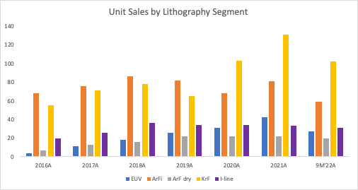
When broken down by various unit sales, there are a few clear trends observable – particularly the relatively stable demand for ArF and ArFi, and I-line products, and a ramp-up in volumes associated with KrF, a trend that has held up into the first 9 months of this year. In addition, steady ramp-ups can be seen in EUV, a trend that should continue to materialize going forwards.
When we start to dig a little deeper into the ASPs (average selling prices) associated with each of these pieces of technology, additional conclusions can be drawn.
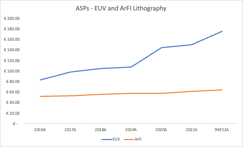
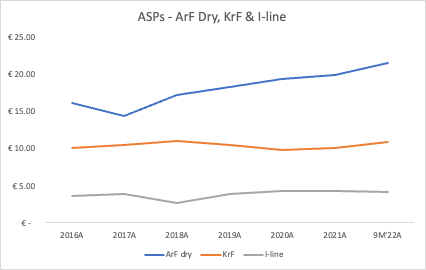
Quite clearly, the continued ramp-up of EUV is of paramount importance to continue scaling their top-line given the ridiculously high ASP relative to other products. In addition, given the monopolistic nature of their positioning in this product segment, they will continue to be able to exert pricing power going forward – since there are no competitive incumbents in sight. The remainder of the products have exerted some degree of price increases, but on average have remained relatively stable over the years.
Classifying the company’s DUV offerings as either Dry or Immersion Systems, we can outline all of the products offered therein.
Immersion Systems:
-
TWINSCAN NXT:2050i – a high productivity dual-stage immersion lithography tool designed for volume production of 300nm wafers at advanced nodes
-
TWINSCAN NXT:2000i – a machine that focused on delivering high-functioning overlay, focus control and cross-matching for high-volume manufacturing of advanced Logic and DRAM nodes
-
TWINSCAN NXT:1980Di – a machine that delivers high degrees of productivity and reliability for volume production at advanced nodes with global system uptime>97%
-
TWINSCAN NXT:1970Ci – a high productivity and image resolution machine that leverages a dual-stage concept design.
Dry Systems:
-
TWINSCAN NXT:1470 – highest productivity lithography platform that exceeds the best-in-class industry standard of 300 wafers per hour
-
TWINSCAN XT:1460K – high productivity dry ArF tool that focuses on providing excellent overlay and imaging performance for volume production at 65nm resolution
-
TWINSCAN XT:1060K – most advanced KrF laser dry lithography system
-
TWINSCAN NXT:870 – leverages latest NXT platform for volume 300mm wafer production at below 110nm resolution
-
TWINSCAN XT:860N/860M – leverages state of the art optics for volume 200 and 300 nm wafer production at below 110nm resolution.
-
TWINSCAN XT:400L – leverages i-line technology, i.e., a mercury vapor lamp, to print features down to 220nm.
On the EUV side of things, the company currently has two main products contained within its portfolio:
-
TWINSCAN NXE:3600D – ASML’s most advanced lithography system that supports volume production at the 5 and 3 nm logic nodes and leading-edge DRAM nodes
-
TWINSCAN NXE:3400C – supports volume production at the 7nm and 5nm nodes.
The company is also focused on continuing to innovate and is directing substantial efforts at their next-generation EUV platform, of which will increase the numerical aperture (NA) from 0.33 to 0.55 NA, denoted as the high-NA EUV machine. High-volume manufacturing of these systems is expected to be fully operational by the end of 2025 and will allow customers to print 1.7X smaller features in comparison to its 0.33NA counterparts!
Outside of the DUV and EUV machines, the company also has products centred around metrology and inspection. Metrology is the science of measurement performed in order to ascertain the dimensions, quality or capacity of something. In semiconductor manufacturing, this typically pertains to procedures associated with using sensors to obtain measurements, of which determine certain physical and electrical properties in wafer processing. Inspection is self-explanatory, but entails the examination of wafers to detect defects of various types ranging from scratches and unwanted particles, to damaged features at each stage of the semiconductor fabrication process flow. These products allow for chipmakers to measure the patterns printed on the wafers to ascertain just how accurate the actual printing process was, and are geared at every stage of semiconductors being brought to market, including R&D to mass production. In addition, using this tech, customers can create automated control loops with process control solutions, optimize lithography systems settings for each exposure to reduce edge placement error, and enlarge the process window to ensure the highest yield and best performance in mass production is achieved. ASML offers customers the following optical metrology and e-beam metrology and inspection systems.
YieldStar Optical Metrology
-
YieldStar 1385 – Optical metrology for in-device overlay that is geared at providing fast and accurate optical metrology for post-etch process monitoring
-
YieldStar 1375F – Fast, accurate in-product overlay and CD metrology for after-etch process monitoring
-
YieldStar 375F – Provides fast and accurate pre-etch overlay and focus measurements for a variety of process conditions.
-
YieldStar 380G – Successor to the 375F machine that is geared at providing even faster and more accurate after-development overlay and focus measurements
E-beam metrology and inspection
-
HMI eScan 1100 – The first multiple e-beam (multi-beam) device for wafer inspection tool, befits a variety of in-line defect inspection applications
-
HMI eScan 1000 – The world’s first multi-beam wafer inspection tool
-
HMI eScan 600 – Flexible e-beam inspection solution that detects multiple defect types in one system
-
HMI eP5 – Highest resolution e-beam system, of which offers CD metrology and defect detection for chip development and production manufacturing.
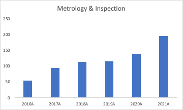
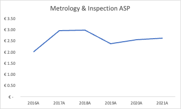
With these product descriptions in mind, we can take a look at how metrology and inspection fits into the company’s business as a whole. Although unit sales have not been disclosed for 9M’22A, from 2016-2021 these were trending positively upwards, all whilst maintaining a steady ASP.
We’ve touched quite a bit on the company’s hardware, but it is also imperative to understand the company’s software positioning as well. Within all of ASML’s lithography machines, they have embedded software, which steers and controls the machines, and whose codebase is comprised of millions of lines of code – a testament to the high degree of moat entrenchment that the company has with their products in general. Software also controls the mechatronic scanner modules within their lithography systems, of which are required to position silicon wafers with nanometer precision for volume manufacturing. This software also helps measure and compensate for nanoscopic inaccuracies that may arise due to material imperfections, or temperature/atmospheric pressure interference and is able to tell the hardware how to correct for these issues as they arise. The company also has application software (off-machine software), which allows for customers to optimize production, calibration, automation etc., and sits below an intuitive user interface. In addition, ASML is also working on software geared at computational lithography – which is a technique that is used to reconstruct the reticle mask and is focused on developing accurate predictions of the semiconductor patterning process.
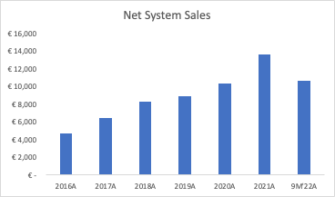
When both the lithography and metrology & inspection systems are viewed together, we arrive at Net System Sales, a value that has compounded at a 23.6% CAGR in between 2016 and 2021, and continues to display strong momentum so far this year:
Net System Sales can also be disaggregated into the various product segments:
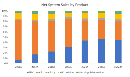
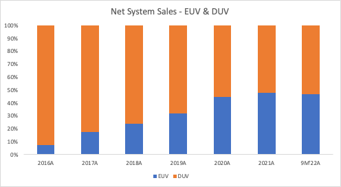
As alluded to earlier, the company is increasingly becoming EUV centric in comparison to DUV, a phenomenon that is likely to be exacerbated heading into the high-NA ramp up anticipated to occur into 2025, even despite the strong projections for DUV demand:
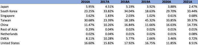
ASML’s customers are global. Despite this diversification, there is no doubt that there is a touch of concentration risk associated with the countries that ASML’s customers inhabit, a phenomenon I will touch upon later, but is outlined below by the geographic distribution of the company’s Net System Sales:
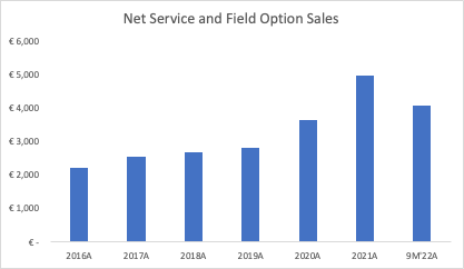
Moving on, System Sales aren’t the only place that ASML generates revenue; they also offer customers a series of Service and Field Options Sales, of which can be thought of as an after-sales support by where ASML engineers provide customers with maintenance services, upgrades/installation of new desired applications, relocations of machines, etc. From 2016 to 2021, this metric grew at an approximate 17% CAGR, a slightly lower tape than its system sales counterpart. Essentially, this metric represents installed base management and should grow proportionally to the company’s installed base.
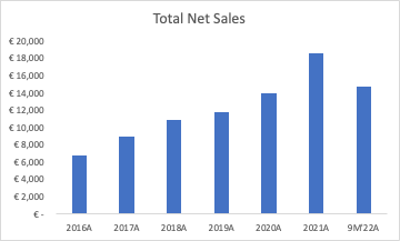
Combined, these values will result in the company’s Net Sales measure, of which came in at approximately €18.61B for 2021, a CAGR of approximately 22%, displaying continued strength this year, and anticipated to be around €21.1B for 2022, a 13.3% YoY increase. This guidance is a drop from the beginning of the year, a result of the company delaying recognition of revenue of €2.2B into 2023. This occurred as a result of “fast shipments”, where instead of testing the functionality of the assembled system in ASML’s facilities and recognizing the revenue upon shipment to the end-customer, ASML ships the assembled machine to the customer and the customer then tests it in their facility, which, when completed, is then recognized by ASML. The process as a whole results in a lengthier recognition process in comparison to the traditional method. In addition, as one would expect, the Net System Sales are the most important part of the business, a phenomenon that has held true over the years.
What do things start to look like when you move towards ASML’s bottom line?
Sticking with the company’s gross profit by segment, for the last few annual periods, Cost of System Sales has been relatively consistent, oscillating between approximately 35-40% of net sales, whereas the Cost of Service and Field Option sales has been moving downwards, settling in at approximately 12.5% of top-line. The result is the following GM profile by segment over the last few years:
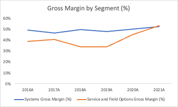
When segments are combined, gross margins have seen relative improvement from 2016 to 9M’22A, but have slightly declined when compared with the full year of 2021:
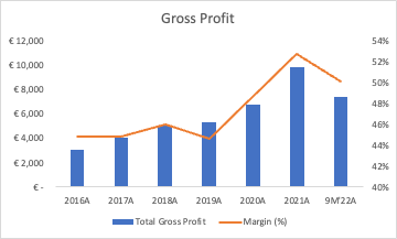
A result of inflationary pressures and supply chain challenges, management anticipates gross margins to approach 50% into year-end. Be that as it may, and as alluded to in Q2, management plans on sharing the extraordinary inflationary costs with customers, and discussions to do so are apparently progressing well, with this inflationary compensation received in 2023, gross profit margins are likely to improve going forward.
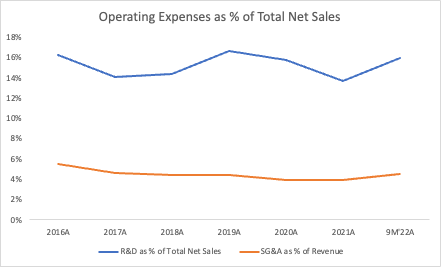
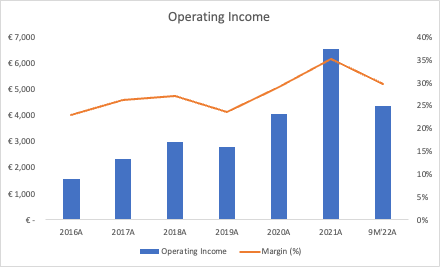
These GP headwinds, when viewed in conjunction with the fact that SG&A (a value that may display some degree of operating leverage and thus improvements in the future), and more importantly R&D (which is likely to remain constant in order for ASML to continue to innovate and maintain competitive positioning) have remained relatively constant in proportion to Total Net Sales. Therefore, operating margins have taken a slight hit when compared with 2021:
Painting a similar tale, Net Income has shown a marked decline YoY:
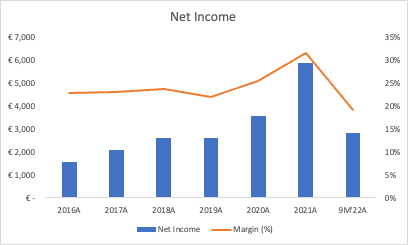
There is no doubt that the company is profitable, impressively so given the nature of the efforts they are directing at creating innovative technologies, however, there will continue to be pressures on the company’s bottom line heading into the end of the year, of which may subside heading into next year if inflation and supply chains are to normalize.
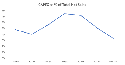
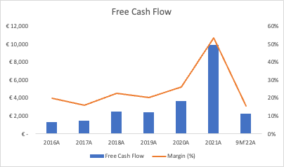
Finishing this section with a discussion of ASML’s capital allocation decisions, the company is surprisingly capex-light, a result of the fact that they work with approximately 4,700 suppliers (as of Q4’21), of whom allocate a large amount of capital on their own to create the plethora of materials and pieces of technology ASML requires within their designs. As a result, FCF margins have historically been in the high teens to mid twenties, values that were exacerbated higher for 2021 due to customer down payments associated with high order intake during that year, but should normalize in the mid-high teens for FY’22 given the headwinds on profits mentioned earlier.
To further illustrate ASML’s financial position, the company has a stable balance sheet. With approximately €3.15B in cash and equivalents as of Q3, and approximately €3.5B in debt. The company’s net debt position of approximately €350M is non-problematic given the degree of profitability the company bolsters.
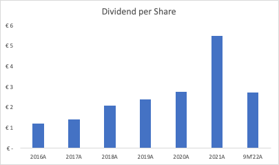
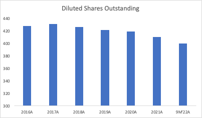
Lastly, the company has had a great track record of returning capital to shareholders via both dividends and buybacks – something they intend to continue to execute upon heading into the future. Heading into the end of December 31, 2025, the company intends to repurchase shares up to an amount of €12B, a phenomenon we will account for in our projections later on:
With this rearview mirror look at ASML in mind, how can we think about the company’s future?
1) The company has unaddressed demand that doesn’t display signs of slowing down.
As I’m sure you are aware, unlike many businesses working their way through the macroeconomic conditions of today, ASML has been dealing with a supply problem rather than weakening demand. In short, they haven’t been able to meet the demand of their customers, a result of the irreplaceable position their technology finds itself in within the semiconductor value chain. Over the last three quarters, the company has registered strong net system bookings and their current backlog stands at an approximately €39B, tremendous growth so far in comparison to 2021:
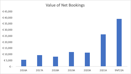
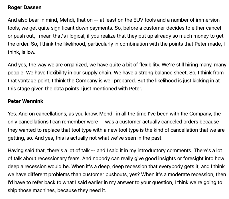
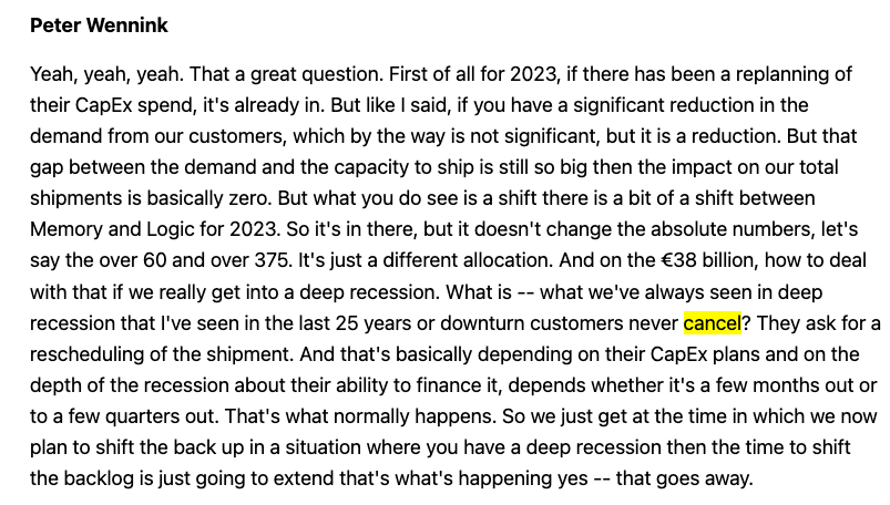
85% of these bookings are either EUV and DUV, and net system bookings for the last three quarters have been a little less than 50% for EUV systems by my calculations – an enticing prospect given both ASML’s market positioning in this area, as well as the fact that these systems are less prone to cancellations given the nature of prepayments, as outlined by Roger Dassen and Peter Wennink on both Q2 and Q3 earnings calls:
In short, there is little indication that economic weakness thus far has resulted in a downturn in future demand – a phenomenon that will need to be continually monitored but is positive for now.
2) The company has strong competitive positioning in their most important product areas and are ramping up production in these areas to meet demand.
As outlined in the company’s most recent investor day, they have strong positioning with respect to their EUV, ArFi and Dry products, with market share that sits at approximately 100%, 90% and 65% respectively and weaker positioning in the metrology and inspection with KLA possessing approximately 60% market share and ASML standing at around 5% according to SA author Robert Castellano’s estimates. EUV is the moat of all moats and is unlikely to change given the fact that incumbents would need to dedicate a decade-plus of development efforts and billions on billions of dollars to even have a shot at taking a percent of market share from ASML. Outside of EUV, the company faces competitive forces on the ArFi front from the likes of Nikon, and dry competition from the likes of Canon. As outlined in the previous sections of the report, looking at the unit sales and ASPs associated with the company’s DUV products, there are no signs of waning under competitive pressures. Heading into the future, I would expect positioning in both ArFi and Dry to continue to improve. There is no doubt that ASML is becoming a full-stack lithography platform, a one-stop shop so to speak that customers can turn to almost everything related to lithography, on both the hardware and software front. I believe this puts them in a much better position than the likes of Canon and Nikon who don’t have exposure to every facet of the lithography market, and should help them gain market share over time. Looking at Metrology & Inspection on the other hand, one could definitely argue that the company has been cutting ASPs to remain competitive. Only time will tell if this is effective.
On another note, the company is ramping up capacity for both DUV and EUV, anticipating to reach capacity of 90 low-NA EUV, 600 DUV systems by 2025-2026, and 20 high-NA systems by 2027-2028, an accretive happening if the company is able to maintain strong positioning and demand, or actions that could result in flooding the market at a time of weakness. Only time will tell how effected ASML with this semi downturn.
On the other hand, there are a few concerns of mine that bear further discussion…
1) Is ASML expensive?
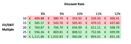
In ASML’s latest investor day, the company outlines their projections for the semiconductor market as a whole. They believe that the market will grow 9% annually between 2020 and 2030, reaching approximately €1.1T in sales by 2025 and 2030. With these market projections, coupled with a few other points outlined throughout this presentation, the company has the following projections for their top-line, gross margins and operating margins. For 2025 they expect: €30-40B in Revenue, 54-56% GMs and 38.2% op-margins (midpoint). For 2030 the company expects: €44-60B, 56%-60% GMs and 42.8% op-margins (midpoint). Using these projections, coupled with a few assumptions of my own, we can take a look at how ASML’s share price might change if the most idealistic of scenarios comes true:
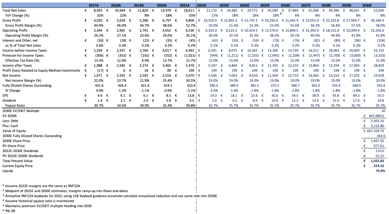
As the above outlines, there is upside potential if everything were to go right per management’s assumptions and if the market were to continue to assign a premium multiple to ASML. However, if this multiple were to compress, due to exogenous factors or otherwise, there would be downside in comparison to the equity price in EUR at the time of writing.
2) Key Risks
ASML has a few notable risks, however, three directly stand out to me – their supply chain, 3D DRAM, and geopolitics as a whole. Starting off with the former, as alluded to earlier, the company has a total of 4700 suppliers. ASML arguably is the endpoint of a complex supply chain, relying on a host of different parties for various components of their lithography machines in order to function. Although this could be said about most modern companies given the still-globalized nature of supply chains, ASML is quite evidently exposed to any potential shortcomings of their suppliers. Take Carl Zeiss as an example, this company is the exclusive producer of optical systems used in ASML’s machines, without them the company would fail to function. Although these risks are mitigated somewhat with exclusivity agreements, black swans impacting various constituents of ASML’s supply chains could be detrimental.
As Dylan Patel alluded to in his analysis of ASML’s investor day, there was no mention about the 3D DRAM developments that could become a serious headwind to demand for lithography in memory end-markets. This technology, which stacks circuitry in a vertical manner (adding an additional plane to the design of memory chips in comparison to 2D DRAM) is being hailed as a potential game-changer for the shortcomings the memory market has been encountering of late, and Samsung (OTCPK:SSNLF) has been devoting serious research at its development, of which has been progressing well. 3D DRAM, though still reliant on lithography, may place more emphasis on etching and other processes, and decrease demands if it were to go completely mainstream. Something to keep in mind going forward.
Lastly, as alluded to earlier, ASML is arguably largely exposed to the geopolitical turmoil associated with chips at the moment. Although ASML argues that the byproduct of heightened concern around the fragility of semi supply chains has resulted in an increase in on-shoring, ASML is exposed to any further actions that the US may take on China, as well as any potential actions China takes on Taiwan. With approximately 40% of revenues attributable to Taiwan, as well as around 15% to China (for 9M’22A), any hostile actions taken by China or the US would have noticeable impacts to not only ASML’s top-line, but likely global economies as well. In addition, the US has already forbade the shipment of EUV machines to China, and has been placing pressure on ASML to stop selling DUV immersion lithography machines as well. Although ASML has gotten around this so far by arguing that DUV immersion technology is relatively old, whose to say what actions the US could take to further dampen China’s progress with semis? Only time will tell.
With all of this in mind, how are you thinking about ASML?
In short, there is no doubt that ASML is one of the most exciting and important companies that has ever existed. Their moat will be hard-pressed to be displaced and they will likely not succumb to an economic downturn the same way other companies will. Be that as it may, the company’s valuation is steep in my eyes and I don’t have 100% confidence in my ability to forecast the direction of the lithography market going forward, especially given the level of uncertainty surrounding semis as a whole right now. I will be monitoring this company for the next few years to see if that ever changes.
Thank you for reading my report.
Disclaimer: The information and research contained herein is all my own opinion and should not be used as a substitute for proper due diligence. Please consult your financial advisor and evaluate your financial circumstances before making any investment decisions.
Disclosure (as of November 29, 2022): MT Capital Research holds no position in the securities discussed herein and does not anticipate to initiate a position in the forthcoming five days.
Editor’s Note: The summary bullets for this article were chosen by Seeking Alpha editors.
Be the first to comment